Simple FM Receiver Circuit Diagram and Connection
Hey, in this article we are going to see a very simple FM Receiver Circuit Diagram. It can be used with a headphone as an output device. FM Receiver is an electronic circuit that receives wireless radio wave signals through its antenna and converts it into usable electronic signals. FM Receiver is also known as FM Radio while it is used as MP3 Player. Generally, it receives an audio signal in the form of radio waves and converts it into an electronic audio signal that drives the speaker so we can hear the music. The circuit diagram shown here is a very simple and cheaper circuit built with very few electronic components. This circuit can be operated with a small battery so it is best suitable for portable FM Radios.
Components Required
- IC BF494 - 2 PCs
- IC LM386 - 1 PCs
- 10K Preset - 1 PCs
- 22pF Trimmer Capacitor - 1 PCs
- 4 Turn 18 SWG Air Core Inductor - 1 PCs
- Ceramic Capacitor 0.22uF- 1 PCs, 0.1uF - 1 PCs
- Resistor 22K - 1 PCs
- Electrolytic Capacitor 25V, 220uF - 1 PCs
- Antenna
- 3.3V to 6V DC Power Supply
Circuit Diagram
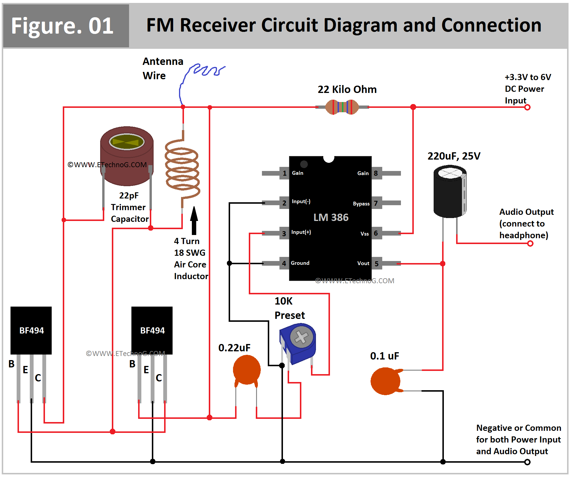
Here, you can see the circuit diagram of an FM Receiver Circuit and its internal component connections.
Connection Procedure
- Connect pin no 6(Vcc) of the LM386 IC to the positive terminal of the power source.
- Connect pin no 2(-input) and pin no 4(ground) of the LM386 IC to the negative terminal of the power source.
- Connect a 0.1 uF ceramic capacitor between pin no 5(Vout) of the LM386 IC and the negative terminal of the power source.
- Connect a 220uF electrolytic capacitor in series with pin no 5(Vout) of the LM386 IC and the audio output terminal.
- Connect the Collector terminal of the first BF494 transistor and the Base terminal of the second BF494 transistor to the positive terminal of the power source in series with a 22 Kilo Ohm resistor.
- Connect the Base terminal of the first BF494 transistor and the Collector terminal of the second BF494 transistor together.
- Connect a 22pF Trimmer Capacitor between the Collector and Base Terminal of the first BF494 transistor.
- Connect the 4-turn 18 SWG air core inductor in parallel with the trimmer capacitor.
- Connect pin no 3(+input) of the LM386 IC to the middle or output terminal of the 10K Preset.
- Connect the Ground terminal of the Preset to the negative terminal of the power source.
- Connect the Power terminal of the Preset to the Base terminal of the second BF494 transistor in series with a 0.22uF Ceramic Capacitor.
- Connect the Emitter terminal of the both first and second BF494 transistors to the negative terminal of the power source.
- Connect the Antenna to the collector terminal of the first BF494 transistor.
Operation and Working Principle
Here, the antenna is used to receive the radio signal. Actually, there are so many different frequencies of signals that are traveling wirelessly. The trimmer capacitor is used to set the desired frequency at which the antenna will receive the desired signal from all the signals traveling wirelessly. The received radio wave signal is converted into a usable electronic signal through the BF494 ICs. The IC LM386 is an operational amplifier IC. It amplifies the audio signal so it can drive the output speaker. Remember that this circuit can drive very low-power speakers. It is best to use it with headphones.
Read Also:
Thank you for visiting the website. keep visiting for more updates.
Simple FM Receiver Circuit Diagram and Connection
 Reviewed by Author
on
April 25, 2023
Rating:
 Reviewed by Author
on
April 25, 2023
Rating:

